


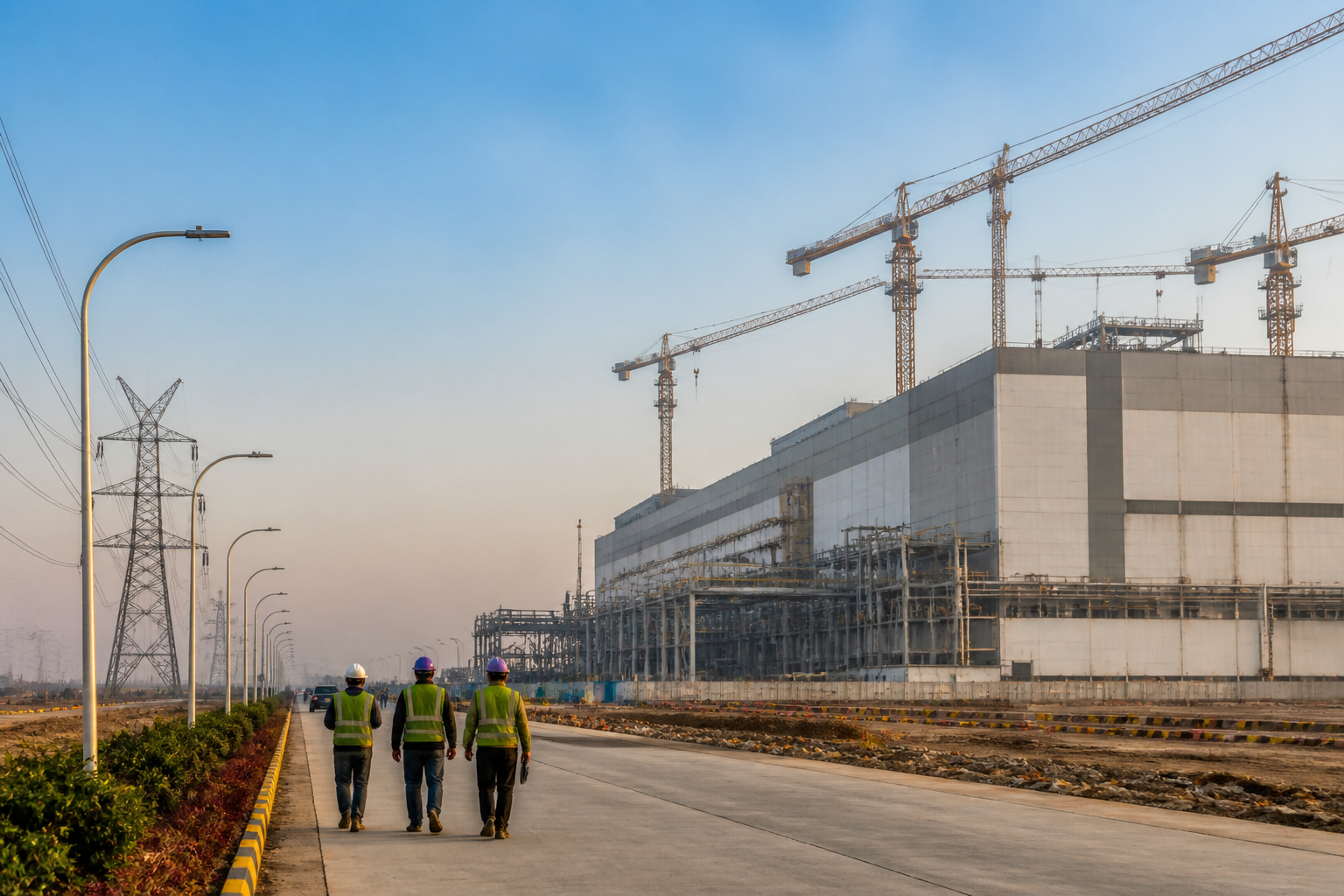
The plan to develop Noida and the wider Gautam Buddh Nagar region as Uttar Pradesh’s first semiconductor-focused district is not only an industrial investment proposition. It is also a test of whether the region can provide the land, water, power, skills and institutional coordination required by one of the world’s most infrastructure-intensive manufacturing sectors.
Under Uttar Pradesh’s Semiconductor Policy-2024, Gautam Buddh Nagar has been designated as the state’s first semiconductor-focused district. According to a report by Navbharat Times, the policy provides for land-related support, financial incentives and other concessions for companies investing in semiconductor manufacturing. The Industrial Development Commissioner has also approved a proposal submitted by the Noida Authority to implement the policy.
The move comes as India’s semiconductor demand is expected to expand significantly. The report cites an estimate that the country’s semiconductor market could reach approximately $110 billion by 2030. It also identifies Taiwan, China and the United States as major global exporters in the sector. For Noida, the policy creates an opportunity to move beyond its existing industrial and technology profile, but it also exposes the limits of the region’s present land and infrastructure capacity.
The immediate constraint is land. The report states that land availability within the Noida Authority area is limited. As a result, the Dadri-Noida-Ghaziabad Investment Region, or DNGIR, where ‘New Noida’ is being developed, is being considered as a potential location for semiconductor-related industries.
That detail is significant because it shifts the semiconductor question from a city-level industrial policy issue to a regional planning challenge. If manufacturing units are distributed between established Noida and the emerging investment region, the success of the policy will depend on more than individual land allotments. It will require reliable connections between industrial sites, workers, suppliers, training institutions and urban services. The supplied report does not establish the final locations, project sizes or construction schedules of specific semiconductor units, but it indicates that the administration is examining a larger spatial footprint for the sector.
Noida semiconductor hub and the infrastructure question
Semiconductor manufacturing requires dependable industrial services. The Uttar Pradesh policy, as described in the report, includes arrangements for adequate water supply and uninterrupted electricity for semiconductor industries. These provisions are central to the policy because the availability of land alone does not make a location suitable for advanced manufacturing.
For Noida and New Noida, the promise of reliable utilities raises questions about how new industrial demand will be integrated with regional infrastructure. The report does not provide capacity figures for water supply, power generation, transmission, distribution or wastewater treatment. It also does not specify whether new utility systems will be built exclusively for semiconductor units or integrated into wider industrial infrastructure.
Those details will matter during implementation. A policy may provide financial support to attract investment, but manufacturing operations will still depend on the physical systems that deliver water and power consistently. The infrastructure challenge is therefore not limited to announcing incentives. It involves coordinating industrial land, utility networks and the administrative agencies responsible for approvals and operations.
The proposed geographical expansion towards DNGIR also makes sequencing important. New industrial areas typically require roads, drainage, water networks, electricity infrastructure and supporting services before large-scale production can begin. The source report confirms that New Noida is being considered as a possible option because of land constraints in Noida, but it does not yet establish the implementation schedule for these supporting systems.
Subsidies can attract investment, but implementation will determine outcomes
The policy provides for subsidies of up to 75 per cent for eligible industrial investment on land measuring up to 200 acres, according to the report. It also offers financial assistance for patent registration: up to Rs 10 lakh for national patents and up to Rs 20 lakh for international patents.
These measures cover two different parts of the semiconductor ecosystem. The land-linked subsidy is intended to reduce the cost of establishing industrial units, while patent assistance is designed to support research and innovation. The policy also proposes assistance through the Chief Minister’s Internship Programme and specialised training programmes in the state’s technical institutions.
Together, these provisions show that the policy is not limited to factory construction. It attempts to address investment, research and workforce preparation. However, the report does not clarify the eligibility conditions, approval process, disbursement timelines or budgetary allocation behind the incentives. It also does not identify the number of companies that have applied for or received support under the policy.
That distinction is important. A policy announcement describes the framework available to investors; it does not by itself demonstrate that production capacity has been created. The report says semiconductor-related industrial units are being established or planned in and around Noida, but it does not provide company-wise details, project costs, employment commitments or commissioning dates. These will be necessary indicators for assessing whether the policy has moved from intent to implementation.
New Noida’s development model faces a new industrial test
The possible role of New Noida places the semiconductor policy within the wider evolution of the DNGIR. The region is being developed as an investment area, and the report identifies it as a potential alternative for industries that cannot secure adequate land within the existing Noida Authority area.
This could give New Noida a specialised industrial role, but it could also increase pressure on the region to deliver services before the arrival of major manufacturing activity. Industrial development and urban development will need to progress together. Workers require housing, transport and daily services, while companies require logistics, utility reliability and predictable approvals. The source material does not provide details of planned housing, public transport or social infrastructure in the investment region, so the extent of this preparation remains unclear.
The regional employment implications are also yet to be quantified. Vipin Kumar Malhan, president of the Noida Entrepreneurs Association, told Navbharat Times that investment by semiconductor companies could spread from Noida to New Noida, covering the DNGIR area. He said the Noida Authority and related organisations would be responsible for providing necessary facilities and supporting the operation of the industrial units.
His assessment points to the need for coordination between the development authority, state departments and industry bodies. Semiconductor manufacturing does not operate as an isolated land-use category. It requires a network of suppliers, specialised workers, research activity and industrial services. Whether those linkages develop locally or remain dependent on other regions will affect the economic value created within Gautam Buddh Nagar.
The policy’s workforce promise remains untested
The policy’s reference to internships and specialised training acknowledges a central challenge: semiconductor manufacturing requires skills that cannot be created through land incentives alone. The report says technical institutions in Uttar Pradesh will organise special training programmes connected to semiconductor manufacturing, while the Chief Minister’s Internship Programme will support the availability of skilled human resources.
At present, the supplied material does not specify which institutions will participate, what courses will be offered, how many trainees will be covered or whether companies will be involved in designing the programmes. It also does not establish whether the training will focus on chip fabrication, testing, packaging, equipment maintenance, design, clean-room operations or other parts of the semiconductor value chain.
This gap matters because the employment effects of the sector will depend on the type of projects that arrive. The report refers broadly to direct and indirect employment opportunities, but does not provide an estimate. Without project-level commitments and workforce data, the employment promise remains a policy objective rather than a measured outcome.
What the Noida semiconductor hub can and cannot establish yet
The available evidence confirms that Uttar Pradesh has created a policy framework for semiconductor investment, designated Gautam Buddh Nagar as its first semiconductor-focused district and approved the Noida Authority’s proposal to implement the policy. It also confirms the broad incentives described by the report, including land-related support, subsidies of up to 75 per cent on up to 200 acres, patent assistance and provisions related to water, electricity and workforce development.
What remains unestablished is equally important. The report does not identify confirmed production facilities, final land parcels, investment values, construction timelines, utility capacities or committed employment numbers. It also does not show how the policy will be funded in practice or how responsibilities will be divided among the Noida Authority, state agencies, technical institutions and industry participants.
The semiconductor plan therefore represents a significant industrial direction for Noida, but its urban consequences will be determined by implementation. The next milestones to watch are specific project announcements, land allotments, utility plans, training partnerships and evidence that New Noida’s infrastructure is being developed in step with the industrial ambition. Until those details emerge, the policy is best understood as a framework for regional transformation rather than proof that a fully operational semiconductor hub already exists.
