


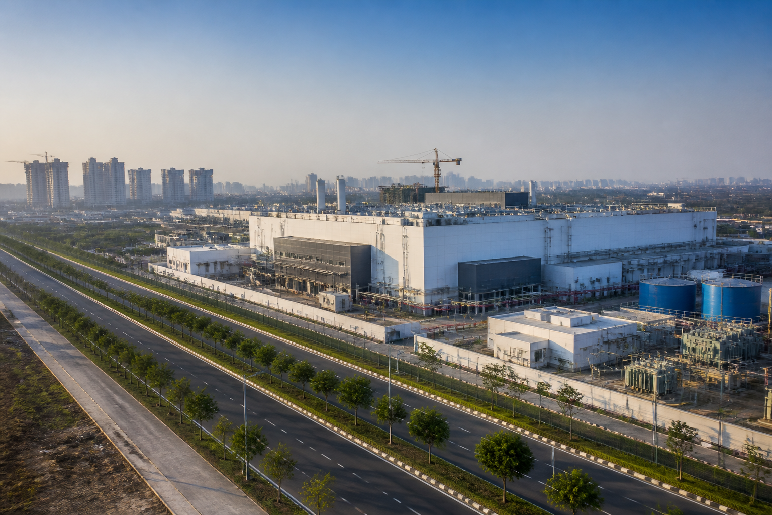
The decision to position Gautam Buddh Nagar as Uttar Pradesh’s first semiconductor-focused district is more than an industrial branding exercise. It places Noida and the proposed New Noida within a national effort to build domestic chip-making capacity, while forcing the region to address a difficult urban question: whether its land, water, power and skills systems can support highly specialised manufacturing at scale.
Uttar Pradesh’s Semiconductor Policy-2024 provides the framework for this shift. Under the policy, companies investing in semiconductor-related manufacturing can receive land, financial incentives and other facilities. The policy was approved in January 2024, and Gautam Buddh Nagar was subsequently designated as the state’s first semiconductor-focused district. According to the report, Uttar Pradesh became the fourth state after Gujarat, Odisha and Tamil Nadu to introduce a semiconductor policy.
The immediate significance for Noida is that the district is being treated as an industrial ecosystem rather than simply another location for individual factories. The policy covers land allocation, financial support, utilities, intellectual property and workforce development. That combination matters because semiconductor manufacturing depends on more than the availability of an industrial plot. It requires reliable electricity, adequate water, specialised technical skills and administrative systems capable of supporting complex production facilities.
The policy’s land provisions are particularly important in a region where available industrial land is limited. The report says the proposed New Noida, being developed under the Dadri-Noida-Ghaziabad Investment Region, is being considered as a potential location for semiconductor industries. The area could therefore become the spatial extension of Noida’s existing industrial economy, allowing large manufacturing units to locate beyond the built-up authority area.
This also creates a planning challenge. The report states that the policy provides subsidies of up to 75 per cent for land parcels of up to 200 acres. However, it does not specify the precise eligibility conditions, the form in which the subsidy will be delivered, the number of companies expected to benefit or the implementation timeline for individual projects. Those details will determine whether the provision produces actual manufacturing capacity or remains an investment incentive on paper.
The reported approval of Noida Authority’s proposal by the state’s Infrastructure and Industrial Development Commissioner is an important institutional step. It indicates that the state-level policy is being translated into an authority-level implementation framework. Yet the report does not detail the administrative process that prospective companies will follow, the agencies responsible for clearances or the service standards for providing land and utilities.
That institutional coordination will be central to the outcome. A semiconductor cluster would involve the state government, Noida Authority, the agencies developing New Noida, utility providers, technical institutions and industrial investors. The policy’s success will depend on whether these institutions can work through a single, predictable process for land allotment, approvals, infrastructure delivery and operational support.
Utilities are another decisive part of the proposed model. The report says semiconductor industries will be provided adequate water and uninterrupted electricity. These are not ordinary industrial requirements. The scale, reliability and quality of utility supply can influence where advanced manufacturing units are located and whether they can operate continuously. However, the supplied material does not provide capacity figures, proposed water sources, electricity infrastructure plans or the financial responsibility for creating and maintaining these services.
For New Noida, this means semiconductor manufacturing could influence the way the emerging investment region is planned. Industrial land would need to be connected not only to roads and power networks, but also to supporting services and worker mobility. The article does not provide details about transport links, housing, logistics facilities or environmental safeguards. As a result, the current evidence establishes the policy intent but not the complete urban infrastructure model required for implementation.
The employment promise is similarly broad but significant. The report says new semiconductor units could create direct and indirect jobs in Noida and New Noida. The policy includes support through the Chief Minister’s Internship Programme and proposes specialised training at technical institutions to prepare workers for semiconductor manufacturing. This suggests that workforce development is being treated as part of the industrial policy rather than as a separate education concern.
The effectiveness of that approach will depend on how closely training programmes match industry requirements. Semiconductor manufacturing is a specialised field, but the supplied report does not identify the occupations involved, the institutions selected, the number of trainees proposed or the scale of employment expected. Without those details, the employment impact cannot yet be quantified. What can be established is that the policy recognises skills as a necessary component of the proposed cluster.
The intellectual property provisions point to a second intended dimension: moving beyond assembly and attracting research and innovation. The policy provides financial assistance of up to Rs 10 lakh for national patents and up to Rs 20 lakh for international patents, according to the report. These incentives are designed to support companies working on research and innovation in the semiconductor sector.
Patent support alone, however, does not establish a research ecosystem. The article does not identify research centres, university partnerships, laboratories or existing semiconductor design companies in Gautam Buddh Nagar. It therefore remains unclear whether the district’s emerging role will focus primarily on manufacturing, component-related activity, research, or a combination of these functions.
The wider economic argument is built around India’s expected growth in semiconductor demand. The report cites an estimate that the Indian semiconductor market could reach approximately 110 billion dollars by 2030. It also identifies Taiwan, China and the United States as major global semiconductor exporters. In this context, the Uttar Pradesh policy is part of a broader effort to expand domestic production and reduce dependence on imports.
The market estimate explains the policy’s urgency, but it does not by itself guarantee that a particular industrial region will attract viable projects. Companies will assess land costs, utility reliability, logistics, technical labour, supply chains and policy certainty. Noida already has an established industrial and technology base, while New Noida offers the possibility of larger land parcels. The report presents these as advantages, but it does not provide comparative figures or confirm investments by named semiconductor manufacturers.
The statement from Noida Entrepreneurs Association president Vipin Kumar Malhan that investment could spread from Noida to New Noida reflects the expectation of local industry. He also said the Noida Authority and related organisations would be responsible for providing necessary facilities and supporting operations. This highlights the role of local institutions, but it is an industry association assessment rather than confirmation of a project pipeline.
The urban implications extend beyond factory gates. If semiconductor-related units are established, the region could see demand for specialised workers, supporting suppliers, logistics services and technical facilities. That could affect industrial land values, commuting patterns and the need for worker housing. None of these outcomes is confirmed in the supplied report, but they are the types of planning pressures that would accompany a successful industrial expansion.
The central evidence at this stage is therefore about policy architecture, not completed investment. Gautam Buddh Nagar has been designated as Uttar Pradesh’s first semiconductor-focused district; the state policy offers land-related and financial incentives; New Noida is being considered because land in the existing Noida Authority area is limited; and the framework includes water, power, patents and skills. The report does not establish how many units will be built, when production will begin or how much public infrastructure will be required.
For Noida, the proposed semiconductor hub will ultimately be tested through implementation. The next meaningful indicators will be the publication of detailed operating guidelines, land allotments, confirmed company investments, utility plans, training partnerships and project timelines. Until those steps become visible, the policy marks a significant direction for the region’s industrial development, but not yet a completed manufacturing transformation.