


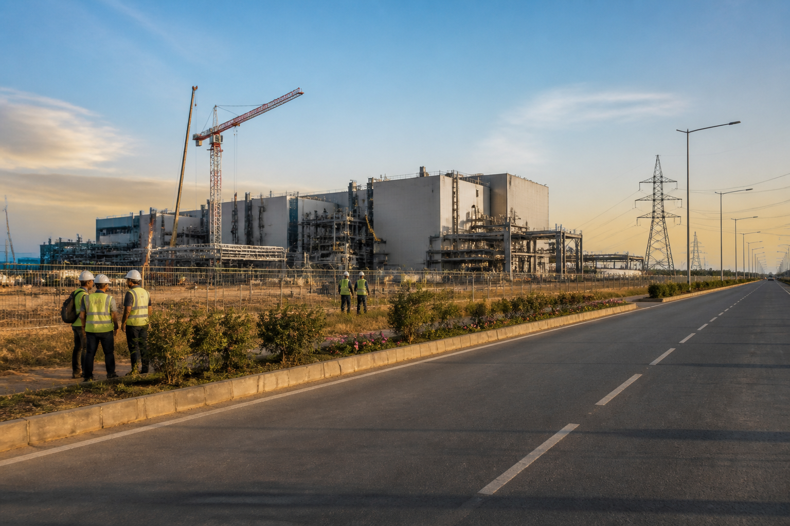
Semicon India 2026 has presented India’s semiconductor manufacturing push as more than a technology-sector expansion. The three-day conference at Yashobhoomi in Dwarka brought together representatives from countries including Japan, Germany, Taiwan and the Czech Republic, with discussions focused on India’s move from chip design into fabrication and assembly. The larger urban consequence is that semiconductor capacity will require new industrial corridors, specialised logistics, dependable utilities and carefully planned employment centres around manufacturing plants.
India already has a strong position in semiconductor design. The report states that more than 20 per cent of the world’s semiconductor design workforce is based in India and that design centres of almost every major fabless company are active in the country. The next phase is materially different. Fabrication and assembly depend on controlled environments, high-purity inputs, uninterrupted power, advanced waste treatment and a supply network that can move sensitive materials safely.
That transition changes the planning challenge. A design centre can operate within an existing commercial or technology district with comparatively limited physical infrastructure requirements. A fabrication plant cannot be treated as an isolated factory. It depends on water-treatment systems, cleanroom air filtration, specialised chemicals and gases, silicon wafers, precision equipment, high-capacity power infrastructure and logistics systems capable of meeting strict handling requirements.
The report identifies plants in Dholera and Sanand in Gujarat, Odisha and Uttar Pradesh as being in the final stages of construction. It does not provide project-wise capacities, investment values or commissioning dates, but the locations indicate the geographic spread of India’s semiconductor ambitions. This is also a shift in the geography of industrial growth. Semiconductor manufacturing is likely to create demand not only within factory campuses but across the wider urban and regional systems that support them.
Semiconductor manufacturing and the new industrial city
The built environment around a semiconductor plant is expected to include industrial corridors, research centres and high-tech townships. The report describes these associated developments as a source of long-term real-estate growth. That claim should be read as an indication of expected demand rather than a quantified market outcome, because no project-level housing, land-price or employment data is provided.
Even without those figures, the institutional implications are clear. Semiconductor projects require coordination between central policy, state industrial agencies, local authorities, utilities, environmental regulators and private manufacturers. The quality of that coordination will determine whether surrounding development becomes an integrated employment and services ecosystem or a collection of disconnected industrial and residential enclaves.
The report’s account of the conference also highlights the importance of supplier networks. A representative from the Czech Republic described semiconductors as a complex ecosystem rather than a single plant, with Europe viewing India as a potential long-term partner for chemicals, specialised equipment and logistics. This places pressure on industrial planning to reserve space and infrastructure for ancillary suppliers instead of focusing only on the headline fabrication facility.
The same logic applies to transport. Sensitive chemicals, gases and silicon wafers require secure and reliable movement between suppliers, plants, warehouses and research facilities. The report refers to a new market for cold-chain logistics, although it does not establish the precise products, network size or operating model involved. The broader point is that semiconductor supply chains require a higher level of logistics coordination than conventional industrial activity.
The infrastructure burden behind chip ambitions
The most significant urban question raised by the report concerns resource intensity. A fabrication plant may require millions of gallons of water each day, while several litres of water may be needed to produce one litre of ultra-pure water. Cleanrooms also require continuous electricity and multi-stage air filtration. The report states that even a microsecond-long power interruption can damage silicon wafers worth crores of rupees.
These requirements make water and power reliability central to the viability of semiconductor clusters. Industrial policy can attract investment through incentives and land, but manufacturing operations ultimately depend on the performance of municipal and regional infrastructure. Water availability, treatment capacity, electricity quality, backup systems and waste-management arrangements become production inputs rather than background public services.
This creates a potential tension between industrial growth and local resource planning. The supplied report does not identify the water sources, allocation arrangements or local demand pressures connected to the proposed plants. It also does not provide details of the power-generation or transmission systems that will serve them. Those gaps matter because the environmental and social performance of a semiconductor cluster cannot be assessed only by the number of plants announced or built.
The report states that the Central Pollution Control Board requires compliance with the Environment Protection Act, e-waste rules and hazardous-waste rules. It also says that new parks require zero liquid discharge and solar grids. A representative of a semiconductor company in Pune said the industry had initially faced concerns around water, electricity and waste management, but that government rules provided a roadmap for green technology and 80 per cent water recycling.
These measures suggest that environmental compliance is being positioned as part of the operating framework rather than as a post-construction correction. However, the material supplied does not include independent assessments of compliance, plant-level recycling performance or the enforcement record of the relevant rules. The distinction is important: a mandated standard, a company commitment and verified performance are different stages of implementation.
From global risk to local governance
The conference discussions linked India’s opportunity to geopolitical risks in the global semiconductor supply chain. Tensions around the Taiwan Strait and recent supply-chain disruptions have encouraged manufacturers and governments to avoid concentrating production in a single location. The report presents India’s democratic system, domestic electronics market and young workforce as factors that could make it an attractive partner.
That external demand creates an opportunity, but it also raises the standard for domestic execution. Global diversification decisions are often made at the level of national policy and corporate strategy, while the practical experience of a semiconductor plant is shaped by local roads, water systems, power networks, waste facilities, housing and worker mobility. The success of the national mission will therefore be visible in ordinary urban systems around each manufacturing cluster.
The distinction between design and fabrication is particularly important for skills and settlement planning. India’s established design workforce provides a base for the sector, but fabrication and packaging require workers who can operate and maintain precision equipment, manage controlled environments and handle specialised materials. The report refers to a young workforce and the potential for high-wage direct and indirect employment, but it does not provide employment estimates or training requirements.
As plants move closer to operation, the relevant question will be whether surrounding cities can provide housing, public transport, healthcare, education and other services for workers and their families. The report’s reference to high-tech townships indicates that private and public actors anticipate this need. Yet township development alone does not establish inclusive urban growth. The relationship between campuses, existing settlements and regional transport networks will determine who can access the new employment centres and at what cost.
What the semiconductor transition reveals
India’s semiconductor strategy is often discussed through the language of technology sovereignty and supply-chain resilience. The urban lens adds another layer: this is also a programme to build specialised industrial cities. Its requirements extend from cleanrooms and laboratories to water-treatment plants, transmission infrastructure, hazardous-material protocols, logistics networks and worker housing.
The report confirms that India is attempting to move beyond its established strength in chip design and enter fabrication and assembly. It also identifies the main implementation pressures: precision, reliable utilities, environmental safeguards, specialised suppliers and coordinated urban development. What remains unclear from the supplied material is the precise schedule, capacity, investment and operational status of the plants mentioned in Gujarat, Odisha and Uttar Pradesh.
Those details will determine whether the current momentum becomes durable industrial capacity. The next milestones to monitor are the completion and commissioning of the announced plants, the performance of their water-recycling and waste systems, the reliability of their power supply, and the emergence of supporting research, logistics and housing infrastructure. India’s semiconductor ambition will ultimately be tested not only inside the factory, but in the cities and regional systems built around it.