


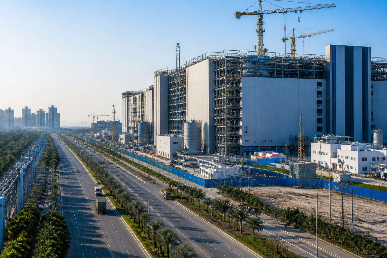
Semicon India 2026 has highlighted a shift in India’s semiconductor ambitions: the country is moving beyond its established strength in chip design towards fabrication, assembly and packaging. The transition is not only a technology story. It is also beginning to shape the infrastructure, industrial corridors, logistics networks, water systems and real-estate markets that will support semiconductor production.
The three-day conference at Yashobhoomi in Dwarka brought together representatives from countries including Japan, Germany, Taiwan and the Czech Republic. Discussions at the event, as reported by Jagran, pointed to a common assessment: India’s manufacturing base is still at an early stage, but its policy direction and project activity are creating the foundations for a larger role in global supply chains.
The report said India currently accounts for more than 20 per cent of the world’s semiconductor design workforce. Major fabless companies already operate design centres in the country, giving India an existing base of technical talent and industry experience. The next challenge is to connect that design capability with the much more demanding physical infrastructure required to manufacture, assemble and package chips.
Projects in Gujarat’s Dholera and Sanand, along with facilities in Odisha and Uttar Pradesh, were described as being in the final stages of construction. The report did not provide project-wise completion dates, production capacities or investment values, but it presented these sites as evidence that India’s semiconductor programme is moving from policy announcement towards industrial implementation.
That distinction matters because semiconductor manufacturing cannot be treated as a conventional factory-development exercise. A fabrication plant depends on tightly controlled environments, uninterrupted utilities, specialised equipment, advanced chemicals and highly reliable logistics. The industrial geography around such facilities must therefore be planned as an ecosystem rather than as an isolated project.
A senior Japanese representative quoted in the report said India’s chip-design experience was of global quality, while maintaining that the central manufacturing challenge would be preserving purity and precision. The representative said cooperation had increased in specialised equipment and ultra-pure technologies, and expressed the view that India could become a major Asian semiconductor hub within five years if the current momentum continued.
The comment identifies a critical difference between designing a chip and manufacturing one. Design centres can operate within existing commercial and technology districts, although they require skilled workers and reliable digital connectivity. Fabrication and packaging plants need a much wider support structure: cleanrooms, power-quality systems, water-treatment facilities, chemical storage, hazardous-waste management, precision equipment maintenance and secure transport routes.
This is where semiconductor development becomes an urban and infrastructure issue. The report said fab plants could lead to the development of advanced industrial corridors, research centres and high-tech townships around them. Such growth could create demand for housing, offices, schools, healthcare, retail and public transport near manufacturing clusters. It could also increase pressure on local roads, freight links, water supply and electricity distribution.
The likely real-estate impact, as described in the report, is therefore tied to employment and infrastructure rather than to a single land transaction. Semiconductor manufacturing is expected to generate direct and indirect employment, including in equipment servicing, logistics, research, chemicals, construction and facility management. However, the supplied report did not quantify the number of jobs or specify the housing requirements of individual locations. Those details will be important in assessing whether surrounding urban development is planned or merely follows industrial investment after the fact.
The global supply-chain context is another important part of India’s strategy. The report linked the push for diversified semiconductor manufacturing to geopolitical tensions in the Taiwan Strait and recent supply-chain disruptions. The underlying lesson, according to the report, is that concentrating production in one location creates systemic risk. Countries and companies are consequently seeking additional manufacturing bases and partners that can offer political stability, a domestic market and a skilled workforce.
India is being presented as one such option because of its democratic institutions, large electronics market and young workforce. A representative from the Czech Republic, also quoted in the report, said semiconductor manufacturing required a complex ecosystem rather than a single plant. Europe, the representative said, viewed India as a potential long-term partner for chemicals, specialised equipment and logistics.
That ecosystem requirement changes how industrial infrastructure must be evaluated. A plant may be completed on schedule and still face operational constraints if chemical supplies are unreliable, if roads cannot safely handle sensitive cargo, or if power interruptions damage production runs. The report said even a microsecond-long power cut could destroy silicon wafers worth crores, underlining the need for power quality and redundancy rather than merely a high installed electricity capacity.
Water is an equally significant constraint. The report said a fab could require millions of gallons of water each day and that several litres may need to be filtered to produce one litre of ultra-pure water. This makes semiconductor clusters heavily dependent on treatment capacity, recycling systems and dependable source water. It also places them in direct relationship with the water demands of nearby cities, industrial users and agricultural areas.
The environmental requirements described in the report indicate that compliance will need to be built into the infrastructure from the beginning. It said the Central Pollution Control Board requires adherence to the Environment Protection Act, e-waste rules and hazardous-waste rules. It also referred to zero-liquid-discharge systems and solar grids as mandatory in new parks, while a representative of a semiconductor company in Pune said the company had a roadmap for green technology and 80 per cent water recycling.
These claims were made in the report by industry representatives and were not accompanied by project-specific compliance documents. Their significance, however, lies in the infrastructure questions they raise. Water recycling, hazardous-material handling and waste treatment cannot remain limited to a factory boundary if a wider semiconductor cluster is to function safely. Local authorities will need to coordinate industrial approvals, utility planning, emergency response and environmental monitoring across multiple agencies.
The logistics system will also be more specialised than the one supporting conventional manufacturing. The report referred to the need to move sensitive chemicals, gases and silicon wafers safely, and said this could create a new market for cold-chain logistics. Such movement requires controlled storage, reliable roads, secure routes and trained operators. The resulting freight demand may influence the design of industrial corridors and the location of warehouses, testing centres and ancillary suppliers.
India’s policy challenge is consequently broader than attracting individual semiconductor projects. It must connect industrial incentives with land-use planning, utility capacity, environmental safeguards, skills and urban services. The supplied report points to activity in Gujarat, Odisha and Uttar Pradesh, but does not set out how responsibilities are divided between the Union government, state governments, industrial development agencies, municipal bodies and utilities. That institutional structure will determine how effectively the proposed clusters are integrated into their regions.
The conference also exposed the difference between announcing a semiconductor ecosystem and delivering one. Construction nearing completion is an important milestone, but it does not establish production at scale. The next indicators will include commissioning, worker training, supplier onboarding, utility performance, environmental compliance and the ability of facilities to maintain the purity and precision required for manufacturing.
For cities, the implications are tangible. Semiconductor hubs can bring high-value employment and research activity, but they can also produce concentrated demand for land, housing, water, electricity and transport. If high-tech townships and industrial corridors are developed together, the benefits may extend beyond factory employment. If residential and civic planning lags behind industrial construction, workers and support businesses may face longer commutes, higher housing costs and uneven access to services.
Semicon India 2026 therefore marks a significant point in India’s industrial transition, but not its conclusion. The evidence supplied in the report confirms a strong design base, projects under construction and growing international interest in India as a semiconductor partner. It does not yet establish the final capacity, operating performance or urban impact of the new facilities. Those outcomes will depend on whether India can deliver the water, power, logistics, environmental systems and surrounding urban infrastructure that semiconductor manufacturing requires.