


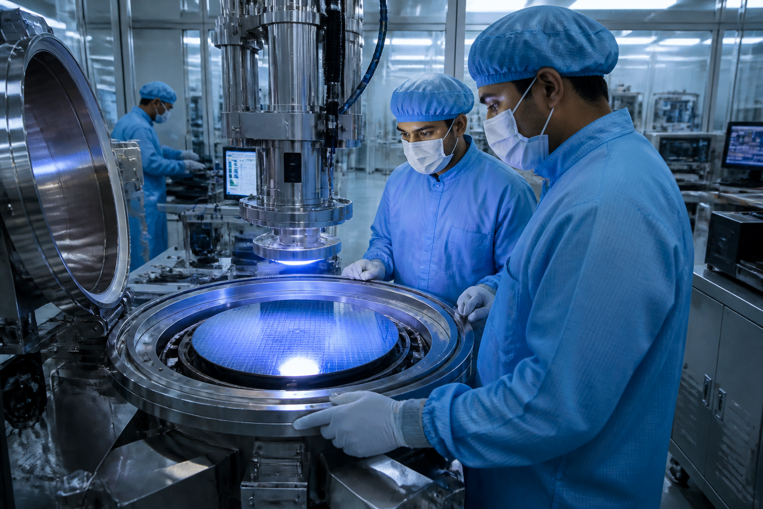
Spintronics AI Semiconductors’ partnership with CSIR-Central Electronics Engineering Research Institute (CSIR-CEERI) signals an important shift in India’s gallium nitride ambitions: the country is trying to move beyond semiconductor design and research towards the harder question of domestic production capacity. The memorandum of understanding signed by the Hyderabad-based company will advance production-ready GaN technology and assess the feasibility of setting up an indigenous GaN fabrication facility in India.
The announcement is significant because the proposed fabrication unit is not being presented as an immediately approved plant or a confirmed investment. Instead, the partnership will examine the technology, infrastructure, fabrication capabilities and possible routes required to build domestic GaN capacity. That distinction matters. In semiconductor manufacturing, the gap between laboratory expertise, product design and an operational fabrication ecosystem is substantial. The MoU places that transition at the centre of the collaboration without claiming that the transition has already been completed.
CSIR-CEERI, a constituent laboratory of the Council of Scientific and Industrial Research, brings two decades of GaN device expertise, according to the statement quoted in the announcement. Spintronics AI brings product-development capabilities and a portfolio of GaN-based products. Together, the institutions intend to create a technology and design transfer framework through which research, process know-how and device design can move from the laboratory into an industry-led manufacturing system.
## The real test is the bridge from research to production
India’s semiconductor debate often focuses on large fabrication plants, investment commitments and supply-chain security. The Hyderabad partnership highlights an earlier and less visible stage: building the institutional bridge that allows specialised research to become manufacturable technology. That bridge involves more than intellectual property. It requires process knowledge, device design, fabrication capabilities, infrastructure planning and a company able to take laboratory outputs towards products.
The source material does not establish that a fabrication unit has received approval, secured funding or entered construction. It says the partners will assess the feasibility of such a facility. The immediate development, therefore, is the formalisation of a joint framework and an evaluation process. Its importance lies in the capabilities being assembled for that evaluation, rather than in a plant already operating or under construction.
Spintronics AI said it is the first Indian company to enter a GaN-focused partnership with CSIR-CEERI. The collaboration is intended to connect the institute’s research base with an industry-led manufacturing ecosystem. That model could help address one of the structural challenges in advanced technology: research institutions may possess specialised knowledge, while companies understand product requirements and commercial development, but neither side alone necessarily provides the full route to domestic production.
For Hyderabad, the partnership also reinforces the city’s role in India’s emerging semiconductor and technology landscape. The company is headquartered in Hyderabad and has operations across India, Canada, Europe and the United States. The announcement does not specify where a future fabrication facility would be located, nor does it provide a project timeline, land requirement, investment size or expected employment figure. Those missing details will be central to judging whether the proposed capacity develops into a substantial industrial project.
## Why GaN matters to the proposed ecosystem
Gallium nitride is described in the announcement as a next-generation semiconductor material with applications across defence, aerospace, space systems, satellite communications, radio-frequency communications, telecom networks, power electronics and electric mobility. These applications span strategic systems, communications infrastructure and energy-related equipment, giving GaN relevance beyond the consumer electronics market.
That range of applications also explains why the partnership is framed around both technology transfer and manufacturing capability. A domestic GaN ecosystem would need to support more than a single product. It would have to connect device research, process development, design expertise and fabrication in a way that can serve different application areas. The MoU’s proposed evaluation of technology needs, infrastructure requirements and fabrication capabilities reflects that wider challenge.
The announcement also cites a market estimate from Spintronics AI founder and chief executive Raghu Varma, who said India’s GaN semiconductor market could grow from about $224 million in 2026 to nearly $1.88 billion by 2033. This is a company-provided estimate, not an independently established forecast in the supplied material. It nevertheless explains the commercial rationale presented by Spintronics AI: expected demand in power, radio-frequency, telecom, defence, space and automotive applications could create a market for indigenous products and manufacturing.
The figures also show why the partners are describing the opportunity as extending across multiple sectors. GaN is not being positioned only as a research material. The company’s stated focus includes analogue, mixed-signal, RF and power semiconductor design, while its portfolio includes proprietary GaN-based products. The proposed collaboration therefore sits at the intersection of specialised material research, product design and industrial capacity.
## Policy alignment does not remove implementation risks
Spintronics AI and CSIR-CEERI have linked the partnership to the India Semiconductor Mission and the Atmanirbhar Bharat push for domestic technology development. This gives the MoU a broader policy setting: reducing dependence on external technology and developing Indian capability in strategically important semiconductor segments.
However, policy alignment is not the same as project execution. The supplied announcement does not identify the financial structure for the proposed fabrication facility, the public support that may be sought, the regulatory approvals required or the institutional division of responsibilities. It also does not say whether the feasibility assessment will result in a plant, a pilot line, a technology-transfer agreement or another form of manufacturing partnership.
Those questions are important because semiconductor fabrication depends on coordinated infrastructure and specialised operational capabilities. The announcement identifies infrastructure requirements as an area for evaluation but does not provide details about utilities, equipment, clean-room systems, supply chains, testing facilities or workforce needs. These should not be assumed from the MoU. They are among the issues that will determine whether the partnership can move from research collaboration to production capacity.
The role of CSIR-CEERI is equally important. Its contribution, as described by the company and the institute, is not limited to general research support. It includes GaN device expertise, process know-how and design knowledge that could be transferred towards industry. The effectiveness of that transfer will depend on how the partners define intellectual-property arrangements, technical milestones and manufacturing responsibilities. The supplied material does not disclose those terms.
## Hyderabad’s opportunity is institutional, not only industrial
The announcement presents Hyderabad as the base of a semiconductor design company seeking to connect Indian research with global product markets. Spintronics AI was founded in 2024 and operates across India, Canada, Europe and the United States. Its stated ambition is to advance next-generation semiconductor technologies, proprietary intellectual property and products from India for global markets.
That model creates a different urban and industrial question from the construction of a single factory. A successful technology ecosystem requires links between laboratories, companies, skilled workers, infrastructure providers and markets. The MoU is an early institutional step in building those links. It does not yet demonstrate the scale of physical development that may eventually follow, but it shows how a city-based design company is attempting to use national research capacity to support a domestic manufacturing objective.
The immediate public-interest value of the development is therefore less about a new building site and more about the institutions being connected. If the feasibility exercise produces a viable pathway, later announcements would need to clarify the location, investment, technology readiness, production scale and implementation schedule. Without those details, the partnership should be understood as a structured attempt to investigate domestic GaN capacity, not as confirmation that India has already established such capacity.
The evidence currently confirms three things: Spintronics AI and CSIR-CEERI have entered a GaN-focused partnership; the collaboration will examine technology, infrastructure and fabrication requirements; and both sides intend to move research and design capability towards an industry-led manufacturing ecosystem. What remains unresolved is whether that pathway will produce a fabrication facility and at what scale. The next meaningful milestones will be the outcome of the feasibility assessment, the terms of any technology transfer and any formal decision on funding, location and construction.