


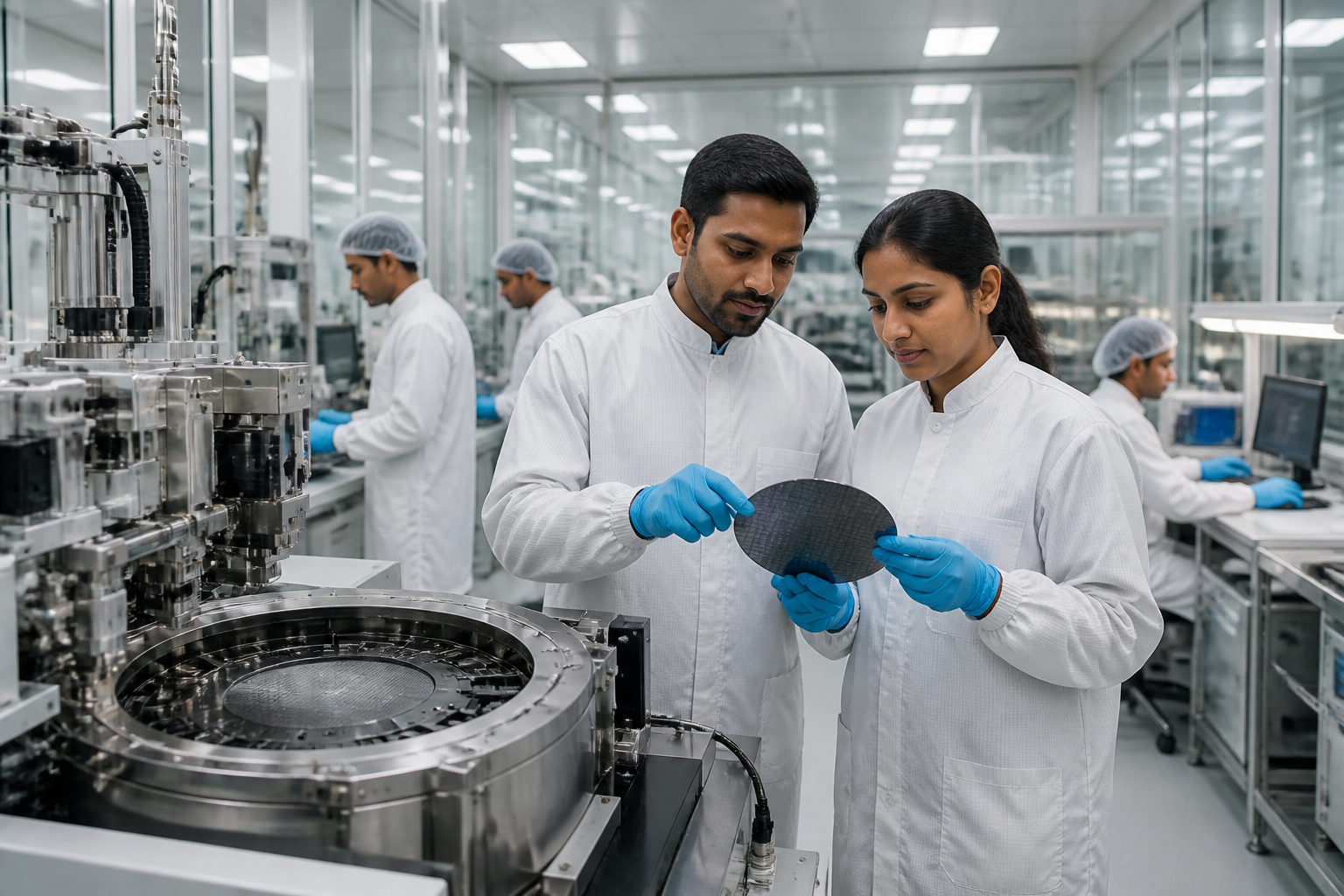
Applied Materials’ plan to invest $5 billion in India over the next decade places the country’s semiconductor ambitions under a sharper test: can research, equipment supply chains and workforce expansion build the industrial capacity needed to support chip manufacturing, even before India has produced a single chip from a large-scale fabrication plant?
The US semiconductor equipment maker announced the investment at SEMICON India in New Delhi, a three-day industry conference covering chip materials, design, fabrication and packaging. More than 600 companies and representatives from 52 countries attended the event, according to the report by Reuters published in Business Standard.
The announcement is significant because Applied Materials operates at a critical point in the semiconductor value chain. Its investment will focus on research, supply chain scale-up and workforce growth rather than announcing a new large-scale fabrication plant. That distinction matters. Semiconductor manufacturing depends not only on fabs, but also on equipment makers, specialised suppliers, engineers, researchers and production capabilities that can support facilities over time.
India’s semiconductor programme is therefore being built through several connected layers. The country is seeking to attract chip manufacturers, packaging companies, equipment suppliers and design capabilities while presenting itself as an alternative location for companies seeking to diversify their operations away from Taiwan and China. Applied Materials’ proposed investment strengthens the equipment and knowledge side of that strategy.
The timing reflects a wider restructuring of the global chip industry. The report describes a scramble for production capacity, intensified by rising demand for computing linked to artificial intelligence and by geopolitical tensions. The United States and China have imposed reciprocal export restrictions on chip technology, while India has positioned itself as a “trusted partner” for companies considering supply-chain diversification.
Prime Minister Narendra Modi said at the conference that the world needed “new and reliable manufacturing locations” and that India was continuously preparing for this role. The statement captures the central policy proposition behind the country’s semiconductor push: India is not only seeking investment in a new industry, but also attempting to establish itself within a strategically important global production network.
## India’s opportunity is larger than fabrication
Government estimates cited in the report project India’s semiconductor consumption to reach as much as $110 billion by 2030. That compares with an estimated $45 billion to $50 billion in 2025. The projected increase provides the demand-side justification for developing domestic capabilities across the semiconductor chain.
Yet consumption and production are different measures of industrial readiness. A large domestic market can attract investment, but it does not by itself create the manufacturing systems, technical workforce or supplier networks required to produce chips at scale. Applied Materials’ decision to centre its India investment on research, supply chains and workforce growth addresses precisely those supporting requirements.
This also explains why the announcement should not be read simply as a measure of fab capacity. Equipment makers are essential to semiconductor production, but their presence does not automatically mean that fabrication capacity is operational. The investment can improve the ecosystem around chip manufacturing while the country continues to work through the more difficult process of establishing large-scale fabs.
That gap is visible in the government’s progress so far. India has committed more than $21 billion across two key semiconductor incentive programmes. Twelve projects have been approved under the incentive programme in the past five years, and three chip-packaging plants, including one operated by Micron Technology, have begun commercial production.
The report also states that India has not yet produced a single chip from a large-scale fabrication plant. The distinction between packaging and fabrication is central. Packaging plants represent progress in the semiconductor chain, but a fabrication facility involves a different level of capital intensity, process complexity and operational dependence on specialised equipment and suppliers.
## The delayed fab exposes the implementation challenge
The country’s marquee fabrication project illustrates the distance between policy approval and industrial output. Commercial production at the $10 billion Tata Electronics fab in Gujarat has been delayed by nearly two years, according to the report.
That delay does not negate the progress represented by approved projects or the start of commercial packaging production. It does, however, show why semiconductor policy cannot be assessed only through investment announcements, project approvals or the size of announced incentives. The more decisive measure is whether projects move through construction, equipment installation, workforce preparation and commercial production.
Applied Materials’ proposed investment could support some of these ecosystem requirements, particularly through research and workforce growth. But the report does not specify the locations, project components, spending schedule or employment numbers associated with the $5 billion commitment. Those details will be necessary to understand how the investment will connect to India’s approved projects and whether it will support operating facilities or primarily build longer-term capabilities.
The institutional design of India’s semiconductor push is already visible in the combination of public incentives and private investment. The government has committed substantial financial support through two programmes, while companies such as Tata Electronics, Micron Technology and Applied Materials are contributing projects and capabilities in different segments of the industry.
This model distributes responsibility across the state and industry. Public policy helps reduce the cost and risk of entering a capital-intensive sector. Companies must then build and operate facilities, develop supply chains and recruit the technical workforce required for production. The resulting ecosystem depends on coordination between incentive programmes, project developers, equipment companies and educational or research capabilities.
## The workforce and supply-chain question
Applied Materials’ stated focus on workforce growth is important because semiconductor manufacturing requires capabilities that cannot be created through buildings and machinery alone. The company’s announcement does not provide a number for planned jobs or describe the training model, so the precise scale of the workforce impact remains unspecified.
Its emphasis on supply-chain scale-up raises a similar issue. The report does not identify the suppliers or materials that would be developed in India, but it establishes that the company intends to expand its presence beyond a narrow investment in one facility. That approach is consistent with the wider requirement for a reliable manufacturing ecosystem, where equipment, materials, research and skilled workers need to operate together.
The urban and infrastructure implications follow from this industrial structure. Semiconductor investment is not limited to a factory boundary. Research facilities, supplier operations and workforce growth create requirements for industrial sites, transport connections, utilities and supporting commercial activity. The supplied report does not provide project-level infrastructure details, so the specific effects on any city or region cannot yet be established. It does show, however, that the investment will be spread across ecosystem functions rather than confined to a single announced fabrication plant.
The location of the Tata Electronics fab in Gujarat gives the semiconductor programme a clear regional anchor, while SEMICON India in New Delhi provided the setting for the latest announcement. The report does not establish where Applied Materials’ planned investment will be deployed. That missing information will be important for assessing how the investment interacts with existing projects and whether the benefits of the semiconductor push are geographically concentrated or distributed across multiple industrial and research locations.
## A stronger test than headline investment
The semiconductor push is now entering a phase in which execution will matter more than ambition. India has a growing projected consumption market, more than $21 billion committed through two incentive programmes, 12 approved projects and three packaging plants in commercial production. At the same time, large-scale fabrication has yet to begin, and the Tata Electronics fab has faced a delay of nearly two years.
These facts point to a mixed but consequential picture. The supporting ecosystem is expanding, and companies are committing capital to research, packaging, equipment and workforce development. The core manufacturing milestone, however, remains incomplete. Applied Materials’ investment can strengthen the capabilities around fabrication, but it cannot by itself demonstrate that India’s large-scale fab model has become operational.
The larger urban-development question is how India will convert strategic industrial policy into durable production capacity. That conversion requires more than land and incentives. It requires coordinated infrastructure, dependable supply chains, specialised skills and institutions capable of sustaining projects through long construction and commissioning periods. The report provides evidence of investment and policy support, but not yet of the full operating system.
The next milestones will therefore be practical: how Applied Materials defines its investment programme, where its research and supply-chain activities are located, how workforce growth is delivered, and whether India’s delayed fabrication projects reach commercial production. Those developments will determine whether the country’s semiconductor ambition becomes a functioning industrial ecosystem or remains primarily a pipeline of projects and commitments.
