


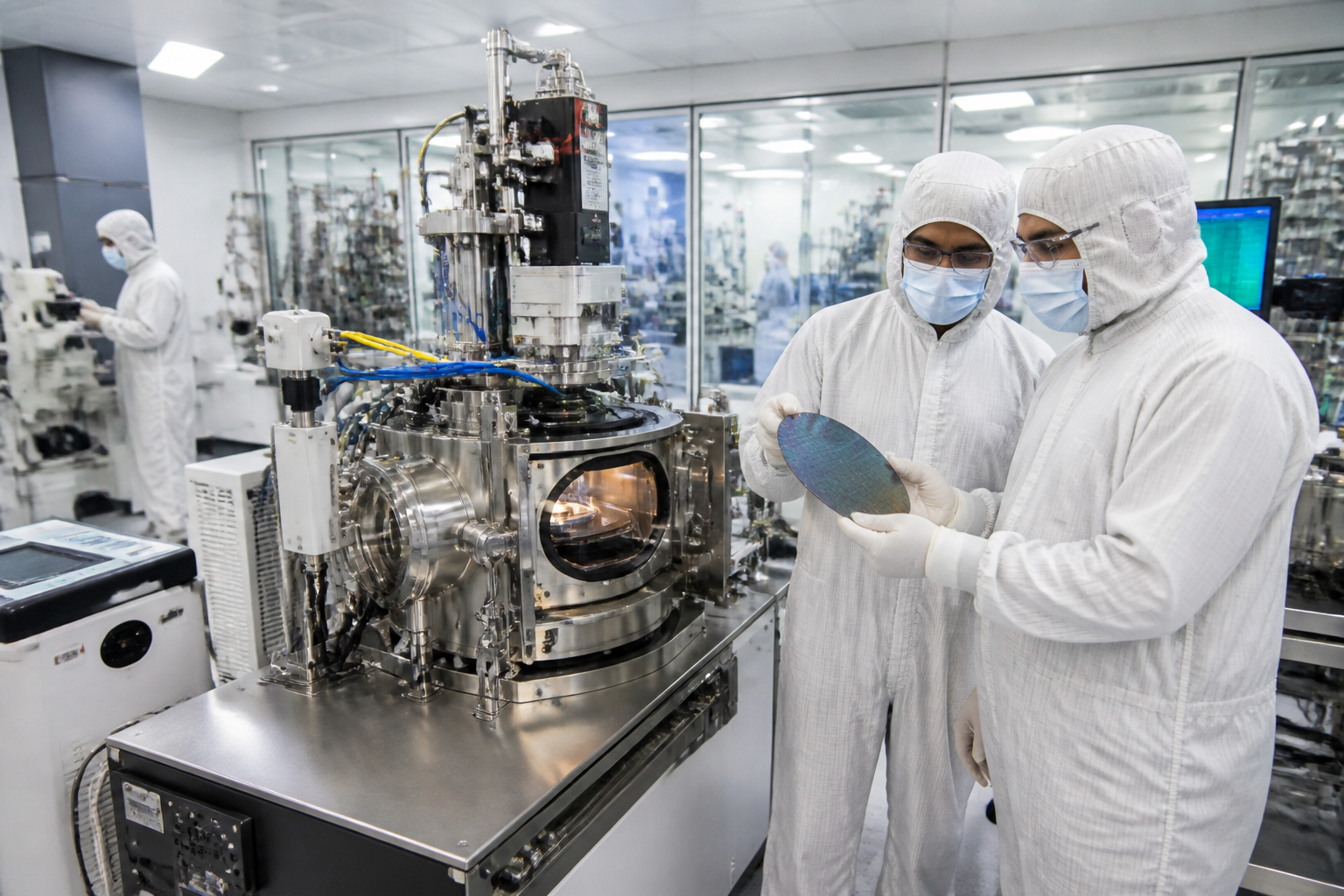
Hyderabad-based Spintronics AI Semiconductors and the CSIR-Central Electronics Engineering Research Institute (CSIR-CEERI) have signed a memorandum of understanding to advance gallium nitride technology and assess the feasibility of an indigenous technology development and fabrication facility in India.
The partnership combines Spintronics’ industry role with CSIR-CEERI’s research capabilities. Under the MoU, the organisations will collaborate on technology and design transfer, with the stated objective of moving gallium nitride research and development closer to an industry-led semiconductor manufacturing ecosystem.
Spintronics said it was the first company in India to enter into such a technology and design transfer partnership with CSIR-CEERI. The two organisations will examine the technology and infrastructure requirements for a potential facility, along with fabrication capabilities and possible pathways for strengthening domestic gallium nitride semiconductor production.
The agreement does not itself announce the construction of a fabrication plant. Instead, it begins a feasibility assessment covering the technical and infrastructure conditions required for such a facility. The supplied announcement does not specify a location, investment value, project capacity, land requirement or commissioning timeline.
Gallium nitride, or GaN, is a semiconductor technology used in applications that require high-frequency or high-power performance. The areas identified in the announcement include defence and aerospace, space systems, satellite communications, radio-frequency communications, advanced telecommunications, power electronics and electric mobility.
The partnership therefore extends beyond a single research programme. Its stated focus is on transferring advanced technology and design know-how from research and development into an industry setting. That transfer is a critical step in any effort to build domestic manufacturing capability, although the announcement does not establish whether the feasibility exercise will lead to a fabrication facility or when a decision could be taken.
Spintronics founder and chief executive officer Raghu Varma said India’s gallium nitride semiconductor market was projected to grow from $224 million in 2026 to nearly $1.88 billion by 2033. He said the initiative could help India capture more of that value domestically. The projection and its source were not detailed in the announcement.
The proposed collaboration also places Hyderabad-based semiconductor design activity within a wider national effort to develop domestic technology and manufacturing capabilities. CSIR-CEERI, based in Pilani, is contributing its research and engineering role to the proposed assessment. Manish Mathew, Scientist F and head of the Diamond Research Group at CSIR-CEERI, said the collaboration would strengthen India’s indigenous GaN technology ecosystem.
The immediate next step is for Spintronics and CSIR-CEERI to evaluate the feasibility, infrastructure needs, fabrication capabilities and potential implementation pathways for the proposed indigenous gallium nitride technology development and fabrication facility.
