


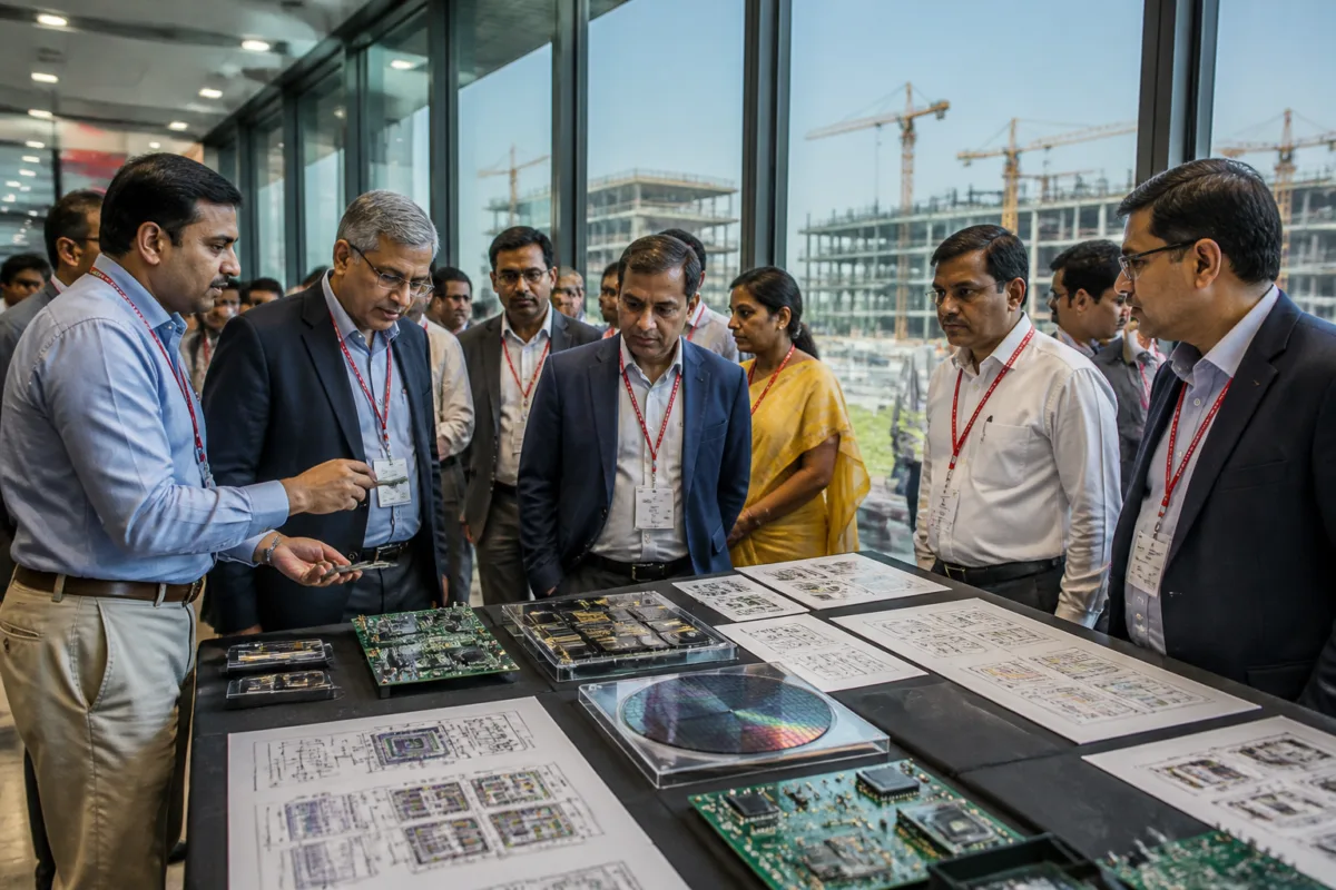
The MP Semiconductor Summit 2026 has placed Indore within Madhya Pradesh’s larger effort to build a semiconductor, photonics and quantum manufacturing ecosystem. The two-day summit, which concluded on Saturday, brought together global technology companies, academic institutions and state officials to discuss AI-driven chip design, advanced packaging, supply-chain integration and specialised skills.
The event’s importance lies less in the summit itself than in the industrial system it seeks to assemble. Semiconductor manufacturing depends on far more than a single fabrication or packaging facility. It requires testing infrastructure, specialised materials, reliable utilities, engineering talent, logistics, certification systems and a network of suppliers capable of meeting stringent quality requirements. The discussions in Indore indicate that Madhya Pradesh is attempting to address these requirements as an interconnected regional manufacturing challenge.
The summit was chaired by Anshuman Raj, managing director of the Madhya Pradesh State Electronics Development Corporation. Industry leaders from Intel, Synopsys, Cadence and Renesas participated alongside experts from IITs and research institutions. Their presence gave the discussions an industry-and-academia dimension, but the report also made clear that the state’s ambition will depend on whether those conversations become physical capacity, supplier relationships and repeatable training systems.
One of the central themes was the relationship between artificial intelligence and semiconductors. Participants discussed how AI-assisted electronic design automation can accelerate circuit design, verification and optimisation of power, performance and area. This can reduce repetitive engineering cycles, but the summit also stressed that human verification remains necessary. The point is significant for emerging manufacturing locations: access to design tools may speed up engineering work, but it does not eliminate the need for experienced engineers, quality-control systems and institutional knowledge.
The relationship works in the opposite direction as well. The growing computational requirements of AI are increasing demand for new processor architectures, higher memory bandwidth and heterogeneous computing. Open hardware frameworks such as RISC-V were also discussed. Together, these trends suggest that Madhya Pradesh is not positioning the semiconductor opportunity only around assembly or conventional electronics production. The summit linked design, packaging, photonics and quantum technologies, although the supplied report does not establish the scale or timelines of any specific investment.
The strongest practical focus was the proposed integration of micro, small and medium enterprises into the electronics and semiconductor supply chain. Participants identified chip packaging, testing, printed circuit boards, speciality chemicals and industrial gases as areas where local capabilities could be developed. These are not peripheral services. They determine how much value remains within the region and whether large anchor manufacturers can source reliably from nearby firms.
For Indore and the surrounding industrial corridor, this creates a more demanding development agenda than simply attracting a large facility. MSMEs entering semiconductor-linked production need access to common testing and certification facilities, specialised industrial clusters and stable relationships with anchor manufacturers. Without those links, local firms may remain outside the most valuable parts of the supply chain, while the state bears the cost of creating industrial land and supporting infrastructure without developing a deeper manufacturing base.
The summit’s recommendation for common testing and certification facilities is particularly relevant to that challenge. Smaller firms may not be able to independently finance expensive equipment or maintain specialised compliance systems. Shared facilities can reduce the entry barrier, but the report does not provide details on their proposed location, ownership, funding or implementation schedule. Those institutional details will determine whether the recommendation becomes an operating industrial asset or remains a conference outcome.
The same question applies to the proposed dedicated industrial clusters. High-technology manufacturing requires more than available plots. It needs dependable logistics, power, water, waste handling, cleanroom-related services and access to trained workers. The report highlights the logistics potential of the Indore-Ujjain corridor and refers to upcoming packaging anchors, but it does not specify the projects, capacities or delivery milestones involved. The next stage of scrutiny will therefore be whether these enabling systems are planned and financed alongside the manufacturing facilities themselves.
Skills emerged as another binding constraint. Summit participants called for localised training in wafer-level packaging, cleanroom maintenance and related specialised fields, as well as stronger links between academic institutions and industry. This reflects the way high-tech manufacturing changes the meaning of industrial employment. A manufacturing cluster requires technicians, maintenance workers, process engineers, quality specialists, testing personnel and researchers. Training that is not connected to actual facilities and production requirements may increase the number of certificates without producing the workforce that companies need.
The emphasis on academic-industry cooperation also connects the proposed semiconductor ecosystem to Indore’s existing institutional geography. The summit included IITs and research organisations, but the supplied material does not identify specific partnership agreements, enrolment targets or training providers. That absence is important because workforce development is a long-cycle investment. It requires clarity about who will train workers, which facilities will host practical instruction and how graduates will move into local employment.
Photonics and quantum technologies broaden the state’s technology agenda. The discussions included international partnerships, including the UK–India trade deal on compound semiconductors, and affordable quantum education simulators such as PARAM Vidya. These initiatives could help expose students and researchers to emerging fields, but the report does not establish whether they are already operational in Madhya Pradesh or were presented as possibilities during the summit. Their contribution should therefore be assessed through concrete partnerships, access and usage rather than through the language of technological ambition alone.
The policy landscape described at the summit combines state-level industrial policy, infrastructure planning and external partnerships. Madhya Pradesh is presented as having progressive policies, logistics advantages and upcoming packaging anchors. Yet the report does not identify the specific policy instruments, public expenditure commitments, land arrangements or regulatory responsibilities behind that positioning. For the state government, the institutional task will involve coordination across industrial development, skills, higher education, logistics, utilities and environmental management rather than the work of a single electronics agency.
That coordination is also the urban question at the heart of the semiconductor push. A technology cluster changes demand for industrial land, housing, transport, education and municipal services. If production and research expand along the Indore-Ujjain corridor, the relevant urban system will include commuting patterns, worker accommodation, freight movement and service infrastructure. The supplied report does not quantify these effects, but its emphasis on logistics, industrial clusters and workforce development shows that the manufacturing strategy cannot be separated from the region’s physical growth.
The summit provides several clear signals but not yet a complete implementation record. It confirms that industry leaders and academic institutions see AI-enabled design, advanced packaging, MSME participation, photonics, quantum technologies and specialised training as connected priorities. It also identifies specific capability gaps, including testing, certification, packaging, PCB production, speciality chemicals, industrial gases and cleanroom maintenance.
What remains uncertain is the conversion of these priorities into funded facilities, identified sites, formal partnerships, production capacities and measurable timelines. For Indore, the success of the semiconductor strategy will depend on whether the city and its surrounding corridor can support the full industrial chain rather than host isolated projects. The next developments to monitor are the creation of common testing infrastructure, the formation of supplier clusters, the status of packaging anchors and the design of localised training programmes.