


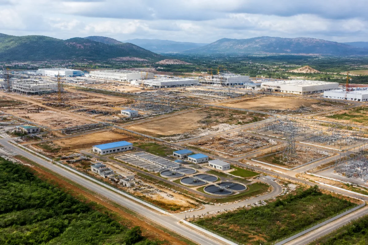
Andhra Pradesh’s decision to offer up to 80 per cent combined capital support for silicon fabrication units, while planning a 5,000-acre semiconductor park at Tirupati, is more than an investment incentive announcement. It is an attempt to assemble the land, utilities, skills, research capacity and administrative machinery that semiconductor manufacturing requires before large-scale production can take place.
The state government has amended its Semiconductor and Display Fab Policy 4.0 to align it with the second phase of the Centre’s India Semiconductor Mission, referred to in the announcement as ISM Semicon 2.0. Under the revised framework, Andhra Pradesh will match central capital support for silicon fabs, display fabs and chip packaging projects, creating a larger combined incentive for eligible investments.
The most visible offer is for silicon fabrication units. The state says these projects can receive combined support of 80 per cent, with 40 per cent coming from the Centre and another 40 per cent from Andhra Pradesh. Other specified fabs and advanced packaging units qualify for combined assistance of 70 per cent, while legacy packaging units can receive 50 per cent support.
These numbers indicate the scale of competition among states to attract semiconductor projects. But the policy also shows that capital support is only one part of the proposed industrial strategy. The state is planning a dedicated semiconductor park at Tirupati with developed land, shared cleanrooms, reliable power, ultrapure water, speciality gases, testing laboratories, logistics, research and training facilities. In semiconductor manufacturing, these are not peripheral amenities. They are part of the operating infrastructure that determines whether an industrial site can support highly specialised production.
The proposal therefore links fiscal incentives with a planned physical ecosystem. A factory may be the most recognisable component of a semiconductor investment, but the park described by the state is intended to provide common facilities for multiple stages of the value chain. Its proposed infrastructure includes both production-support systems, such as cleanrooms and ultrapure water, and institutional facilities, including laboratories, research centres and training infrastructure.
## The policy is building an ecosystem, not only subsidising a plant
The revised policy covers 10 categories across six pillars: design, machines and materials, fabs, packaging, research and development, and talent. That structure matters because it broadens the policy beyond the construction of a single fabrication facility. It places chip design, production equipment, materials, packaging, research and workforce development within the same state-level framework.
For chip design, Andhra Pradesh says it will add 50 per cent of the Centre’s support. Commercial design startups can receive combined seed funding of up to Rs 22.5 crore. The policy also introduces a deployment-linked incentive under which the state adds 4.5 per cent of net sales to the Centre’s nine per cent support, taking the combined assistance to 13.5 per cent, subject to ceilings.
The different forms of support suggest that the state is trying to address more than the initial cost of setting up a plant. Capital-intensive manufacturing requires large upfront investment, while design companies and startups have different funding needs. A sales-linked incentive, meanwhile, ties part of the support to commercial deployment rather than only to the creation of physical capacity.
The policy also covers machines and materials. The state will add 18 per cent of capital cost to the Centre’s 30 per cent support in this segment. Assembly, Testing, Marking and Packaging, or ATMP, and Outsourced Semiconductor Assembly and Test, or OSAT, units will receive matching state capital assistance. This creates a policy bridge between fabrication and the downstream stages that prepare chips for testing, packaging and use.
However, the announcement does not identify any confirmed investor, approved fab or operational project at Tirupati. The 5,000-acre park remains a plan described by the state government. That distinction is important: an incentive framework and proposed industrial infrastructure can improve the conditions for investment, but they do not by themselves establish that a manufacturing cluster has been created.
## Tirupati’s proposed park makes urban infrastructure a central issue
The proposed park would be a large land and infrastructure project, even before the arrival of semiconductor factories. Its stated requirements include developed land, continuous power, ultrapure water, speciality gases, testing facilities, logistics and shared cleanrooms. These systems imply a development model in which the state must coordinate industrial land, utilities, transport and specialised services rather than provide a conventional plot in an industrial estate.
The announcement does not provide the park’s development timeline, land-acquisition status, utility capacity, financing plan or construction schedule. It also does not specify how the proposed facilities will be governed, operated or maintained. Those details will determine how quickly the plan can move from policy announcement to usable industrial infrastructure.
Water and power are particularly significant because the state has explicitly identified reliable power and ultrapure water as part of the park’s planned facilities. These are not ordinary estate services. Their inclusion indicates that the government expects shared infrastructure to reduce the burden on individual investors and make the site more attractive for specialised manufacturing. At the same time, the policy announcement does not quantify demand, supply arrangements or the environmental and operational systems that would support these utilities.
The park’s proposed research and training infrastructure adds another layer to the urban and regional development question. A research centre is initially proposed at IIT Tirupati, while a training centre would offer companies Rs 10,000 per trainee per month for six months. The stated incentive is intended to support workforce preparation, but the announcement does not establish how many trainees would be covered or which occupations and skill levels would be prioritised.
This institutional design could influence whether the park functions as a collection of subsidised units or as a connected cluster. An investor facilitation council is also proposed, suggesting that the state wants a dedicated mechanism to coordinate approvals and investor requirements. Minister Nara Lokesh said the government would provide single-window clearances and match the Centre’s support rupee for rupee to attract investment.
## High incentives come with defined limits
The policy’s headline support of 80 per cent is subject to limits. Andhra Pradesh says its incentives are capped at 50 per cent of eligible fixed capital investment, while assistance from all sources cannot exceed 90 per cent of eligible investment. Mega and ultra-mega projects can receive customised packages.
These conditions show that the headline percentage cannot be read as an unrestricted reimbursement of total project expenditure. The actual support available to an investor will depend on the definition of eligible investment, the applicable project category, the central contribution, the state’s contribution and the ceilings in the policy. The state has also said that the policy will remain valid for five years or until it is replaced, while benefits already granted will continue to be protected.
For public administration, the challenge is therefore twofold. The government must make the promised incentives accessible enough to attract projects, while applying eligibility rules and ceilings that protect the structure of the programme. It must also coordinate support across the Centre, the state and the proposed park institutions. The announcement establishes the broad architecture of that system, but not its implementation record.
The state’s policy also includes research, development and talent projects, for which it will provide 25 per cent of eligible project cost. Combined central and state assistance in this category is capped at 75 per cent. This creates a separate support pathway for capabilities that may not immediately appear as factories but are necessary to sustain design, engineering, testing and research activity.
## The larger question is whether infrastructure can convert incentives into capacity
Andhra Pradesh is presenting its revised policy as a coordinated response to the requirements of the semiconductor industry. Its offer combines large capital incentives with land, shared facilities, institutional support, research infrastructure and training assistance. The policy also attempts to cover several segments, from design and materials to fabrication, packaging and talent.
The evidence supplied with the announcement confirms the scale and structure of the proposed support. It does not yet confirm the number of investors, the investment value, the construction schedule or the operational capacity of the Tirupati park. Those are the measures that will show whether the policy has moved beyond competition for announcements and towards functioning industrial infrastructure.
The next stages to watch are the development of the 5,000-acre park, the creation of the investor facilitation council, the establishment of the research centre at IIT Tirupati, the rollout of the training centre and the approval of projects under the amended policy. Andhra Pradesh’s semiconductor strategy has set out a financial and institutional framework; its effectiveness will depend on how that framework is translated into serviced land, reliable utilities, skilled workers and operating facilities.