


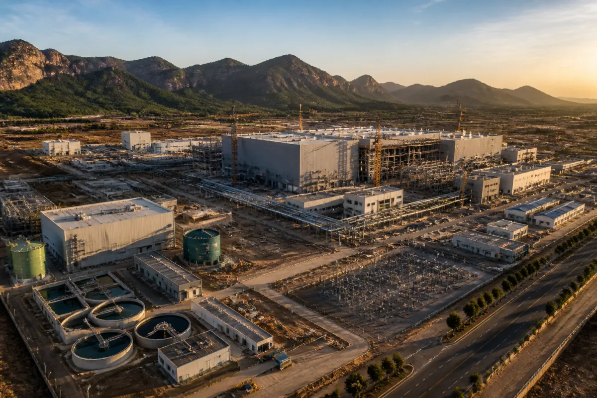
Andhra Pradesh’s amended semiconductor policy is not only an incentive package for chip manufacturers. It is also a proposal to build an industrial ecosystem around Tirupati, combining subsidised capital, developed land, specialised utilities, research institutions and workforce support. The state government says it will offer combined capital assistance of up to 80 per cent for silicon fabrication units while planning a 5,000-acre semiconductor park.
The policy has been aligned with the second phase of the Centre’s India Semiconductor Mission, known as ISM Semicon 2.0. That alignment is significant because semiconductor manufacturing requires more than an industrial plot and conventional factory infrastructure. Fabs and advanced packaging facilities depend on uninterrupted power, ultrapure water, speciality gases, testing systems, cleanrooms, logistics and highly trained workers. Andhra Pradesh is therefore presenting the policy as an attempt to assemble the physical and institutional conditions required for an industry with unusually high entry costs.
The announcement also shows how competition between Indian states is moving beyond the provision of generic industrial land. The revised framework promises state-level support across ten categories and six pillars: design, machines and materials, fabrication, packaging, research and development, and talent. This makes the policy broader than a single-project subsidy. It is structured to cover different layers of the semiconductor value chain, from startups and chip design to manufacturing equipment and workforce training.
At the centre of the package is the proposed capital support. Silicon fabs can receive combined assistance of 80 per cent of eligible project costs, with 40 per cent each from the Centre and Andhra Pradesh, according to the government release cited by PTI. Other specified fabs and advanced packaging units qualify for combined support of 70 per cent, while legacy packaging units can receive 50 per cent. The state government said its proposed support for silicon fabs is higher than incentives offered by several other states.
These figures are politically and industrially important, but they do not mean that the state will finance 80 per cent of every project expense. The policy specifies that state incentives are capped at 50 per cent of eligible fixed capital investment, while assistance from all sources cannot exceed 90 per cent of eligible investment. Mega and ultra-mega projects may receive customised packages. The distinction between eligible investment and total project cost will therefore be central to how the package is ultimately applied.
The state’s approach is based on matching central support. IT Minister Nara Lokesh said the government wanted India to build its chips in Andhra Pradesh and would match the Centre’s support rupee for rupee while providing single-window clearances. The statement identifies two linked objectives: reduce the upfront financial burden for investors and reduce administrative friction during project approvals.
Single-window clearance, however, is only one part of the implementation challenge. A semiconductor park must provide services that are more demanding than those required by many conventional industrial estates. The proposed Tirupati park is expected to include developed land, shared cleanrooms, reliable power, ultrapure water, speciality gases, testing laboratories, logistics, research facilities and training infrastructure. Each of these components will have to be planned, financed, delivered and maintained as part of a functioning industrial system rather than as isolated amenities.
The choice of Tirupati also gives the proposal a regional development dimension. The planned park would occupy 5,000 acres, making land assembly, internal roads, utility networks and environmental management major elements of the project. The supplied report does not establish the acquisition model, construction timeline, financing arrangement or the status of land identification. Those details will determine whether the park becomes a ready-to-use manufacturing cluster or remains primarily a policy proposition until supporting infrastructure is delivered.
The policy’s design support provisions indicate that the state is also seeking activity beyond large fabrication plants. Andhra Pradesh will add 50 per cent of the Centre’s support for chip design, while commercial design startups can receive combined seed funding of up to Rs 22.5 crore. Under a deployment-linked incentive, the state’s 4.5 per cent support added to the Centre’s 9 per cent assistance takes the combined support to 13.5 per cent of net sales, subject to ceilings.
This spread of incentives matters because fabrication, packaging, design and equipment manufacturing have different capital and infrastructure requirements. A state that attracts only a single large fab may gain a high-profile investment without developing a wider local supplier and skills base. By including machines and materials, the policy signals an effort to support the industrial inputs that surround chip production. For these units, the state adds 18 per cent of capital cost to the Centre’s 30 per cent support.
The packaging segment receives a similar treatment. Assembly, Testing, Marking and Packaging units and Outsourced Semiconductor Assembly and Test units are eligible for matching state capital assistance. These facilities are distinct from silicon fabs but form an important part of the manufacturing chain. The policy’s inclusion of both advanced and legacy packaging indicates that Andhra Pradesh is not limiting its offer to the most technologically intensive segment of the industry.
Research and talent support form the third institutional layer. For research, development and talent projects, the state will provide 25 per cent of eligible project cost, with combined central and state assistance capped at 75 per cent. The government is also proposing a research centre initially at IIT Tirupati and a training centre through which companies would receive Rs 10,000 per trainee each month for six months.
The proposed institutions are intended to address a structural problem in industrial policy: capital subsidies can help establish factories, but they do not automatically create the research capacity or workforce needed to operate them. The investor facilitation council would provide a coordination mechanism, while the research and training centres would connect firms with local institutions and potential employees. The supplied material does not yet specify the governance structure, intake capacity or curriculum for these institutions, so their eventual contribution cannot be assessed from the announcement alone.
The policy remains valid for five years or until it is replaced. Benefits already granted will continue to be protected. That provision gives existing beneficiaries some continuity while the state updates its framework to match the next phase of the national mission. It also establishes a defined policy window for new investments, although the report does not provide project-specific commitments, construction milestones or employment targets under the amended policy.
The numbers reveal the scale of the state’s offer but not yet the scale of its outcomes. Up to 80 per cent combined capital assistance for silicon fabs, 70 per cent for specified fabs and advanced packaging, 50 per cent for legacy packaging, Rs 22.5 crore in potential design-startup seed funding and a 5,000-acre proposed park create a substantial public policy proposition. They do not, by themselves, establish how many companies will invest, how much private capital will be mobilised or when production will begin.
That gap between policy capacity and project execution is the central urban and infrastructure question raised by the announcement. Semiconductor facilities require reliable utilities and specialised industrial services at a standard that cannot be improvised after factories are built. They also require transport links, housing and services for workers, institutional coordination and a predictable approvals environment. The proposed park’s success will therefore depend on whether these components advance together.
For Tirupati, the project could connect a major land and infrastructure plan with a high-value manufacturing strategy. But the available information supports only the conclusion that the state has amended its policy and announced the park plan. It does not yet confirm land delivery, construction contracts, utility commissioning, investor commitments or operational dates. Those milestones will be necessary to measure whether Andhra Pradesh’s subsidy-led strategy is translating into a functioning semiconductor ecosystem.
The immediate next steps are the implementation of the revised policy, the development of the proposed investor facilitation, research and training institutions, and further planning for the Tirupati park. The policy will operate for five years or until replaced, while the government’s stated offer remains subject to its eligibility, assistance and investment ceilings.