


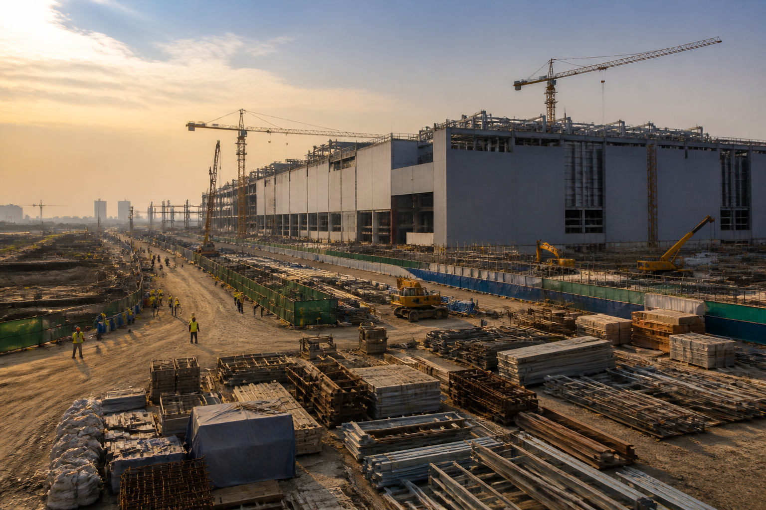
The HCL-Foxconn joint venture will manufacture about 36 million display driver chips a month at its upcoming semiconductor packaging facility in Uttar Pradesh, a capacity the company expects could meet roughly 40 per cent of India’s domestic requirement.
India Chip Chairman Shikhar Malhotra announced the projected capacity while delivering a keynote at Semicon India 2026. The more than ₹3,700-crore facility is being built alongside the upcoming Noida International Airport and is expected to open in 2028.
Prime Minister Narendra Modi virtually laid the foundation stone for the project on Thursday at the Yamuna Expressway Industrial Development Authority area in Jewar, Greater Noida. The facility broke ground in February, according to Malhotra.
The plant will initially focus on display driver chips used in smartphones, laptops, cars, wearables, televisions and medical devices. These chips control the display panels and are used across consumer electronics, vehicle dashboards and medical equipment.
Malhotra said that 80-85 per cent of the components used in an Indian display currently come from outside the country. He also said India buys more than $30 billion worth of chips from abroad every year, describing the import dependence as a domestic supply gap the project aims to address.
The facility will operate as an outsourced semiconductor assembly and test, or OSAT, plant. OSAT facilities package and test semiconductor components after fabrication, forming a critical link between chip manufacturing and the final electronic product. The project’s initial focus on packaging places it within the broader effort to expand India’s semiconductor manufacturing ecosystem.
The company expects the facility to create demand for a wider group of domestic suppliers. These could include manufacturers of substrates, lead frames, bonding wires, moulding compounds, specialty gases and precision tooling. Malhotra said most of these inputs are currently imported.
“Every OSAT pulls a constellation behind it — substrates, lead frames, bonding wires, molding compounds, specialty gases, precision tooling, calibration,” Malhotra said. He added that each commissioned unit could create a customer base that makes it commercially viable for suppliers to manufacture in India instead of importing into the country.
The project’s location near Noida International Airport places it within one of Uttar Pradesh’s emerging industrial and logistics zones. The airport and the Yamuna Expressway Industrial Development Authority region are being developed as part of a wider economic corridor that is attracting manufacturing and infrastructure investment. The semiconductor facility adds a high-value electronics manufacturing component to that industrial geography.
The joint venture also plans to connect the new manufacturing capability with India’s existing strengths in software, artificial intelligence and chip design. Malhotra said nearly one in five chip designers globally is Indian and argued that manufacturing capacity could complement the country’s established engineering and technology base.
The company’s stated milestone is to open the facility in 2028. Until then, the project’s implementation will depend on construction, equipment installation, testing and the creation of the supporting supplier network required for commercial operations.