


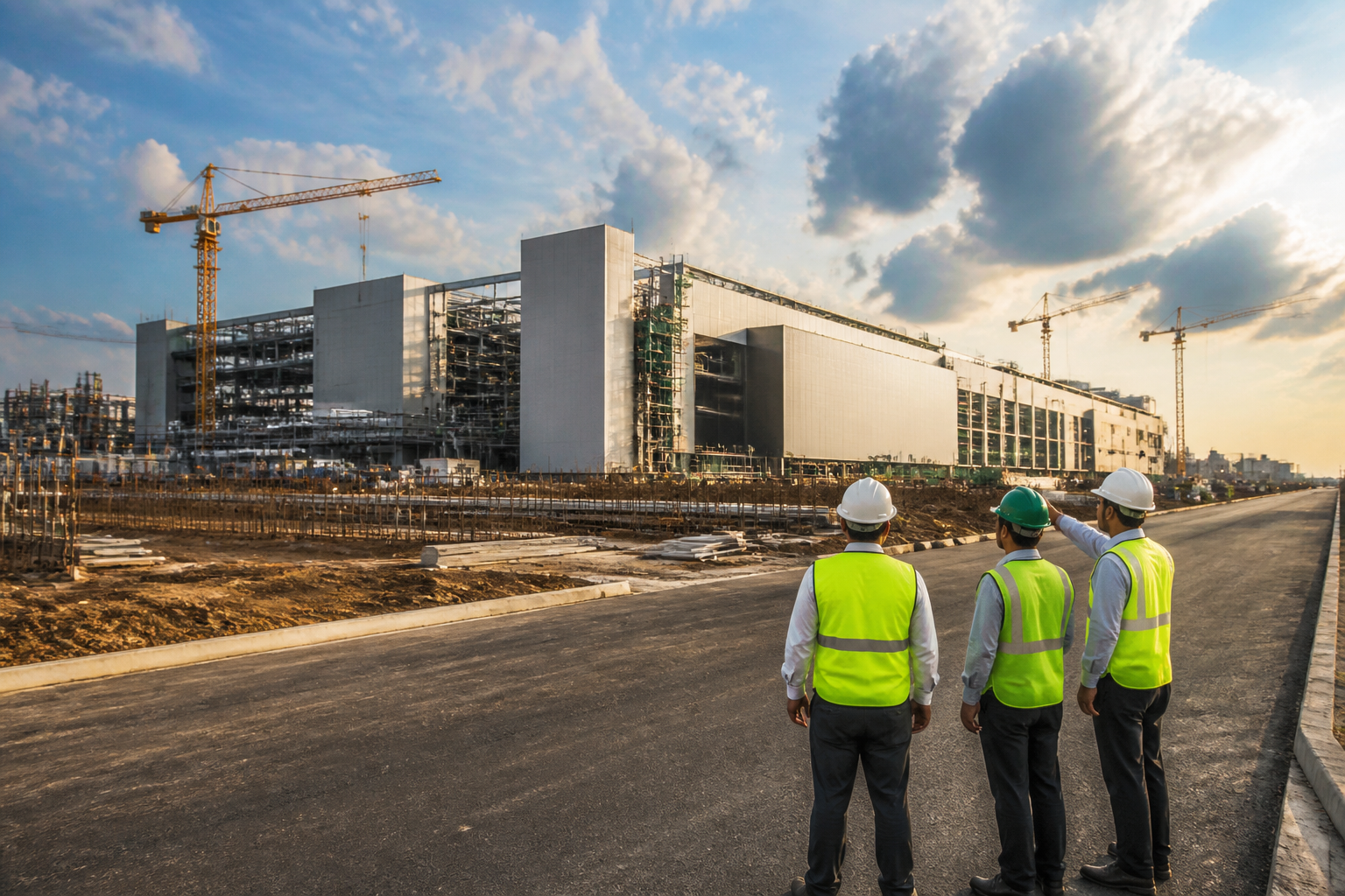
ASML’s planned expansion of its customer-support, supplier and wider ecosystem presence in India signals that the country’s semiconductor ambitions are entering a more demanding phase. The immediate trigger is Tata Electronics’ upcoming 300 mm semiconductor fab in Dholera, Gujarat, but the larger challenge is whether India can build the industrial network required to make one fab operational and then support several more.
The Dutch semiconductor equipment maker’s presence in India has so far been limited, according to Allan Wayne, ASML’s Chief Strategic Sourcing and Procurement Officer. Speaking at SEMICON India 2026, Wayne said the Tata Electronics facility gives ASML a customer base around which it can expand support and develop a broader ecosystem. Earlier this year, Tata Electronics and ASML signed a memorandum of understanding to advance semiconductor manufacturing in India.
That relationship matters because a semiconductor fab is not an isolated factory. It depends on equipment support, qualified suppliers, production processes, quality control and the ability to maintain a demanding manufacturing schedule. ASML’s stated priority is to help Tata Electronics qualify production, achieve good quality and yield, and keep the project on track for its expected operational target in 2028. The company has not, however, announced plans to manufacture equipment in India.
Wayne’s comments draw a distinction between expanding support for a manufacturing customer and creating a local equipment-manufacturing base. ASML currently plans to build its supply-chain presence first. Manufacturing in India could be considered at some point, he said, but there are no such plans at present. That sequence exposes one of the central institutional questions in India’s semiconductor programme: how quickly can domestic manufacturing capacity grow when critical capabilities, suppliers and specialised technical support are still being assembled around the first major projects?
The scale of India’s stated ambition makes the question more urgent. Wayne said India’s semiconductor market could reach $110-120 billion by 2030. He also said the country may need several fabs to meet its production goals, with domestic wafer fabs expected to supply 15-25 per cent of semiconductor demand by 2032 and 35-50 per cent by 2035. Meeting those targets could require a dozen fabs or more, according to his assessment.
These figures indicate that the Dholera project is being treated as a starting point rather than a complete solution. A single facility can establish production capability and create a base of operational experience, but it cannot by itself deliver the domestic share of supply described for the next decade. The transition from one fab to several will depend on whether the ecosystem created around Tata Electronics can be repeated, expanded and made reliable enough for additional projects.
The technology pathway is also broader than a race to produce only the most advanced chips. Wayne said India’s initial semiconductor manufacturing ambitions would be driven by mainstream technologies, including processes at 28 nanometres and above. He identified analogue chips, mainstream logic, power semiconductors, sensors, NAND and advanced packaging as areas where significant innovation remains possible.
That emphasis changes the infrastructure question. India’s semiconductor strategy does not depend exclusively on immediately matching the most advanced global nodes. It also depends on building dependable production for chips used in vehicles, electrification, automation, sensors and other applications. These segments require manufacturing quality, stable supply and timely delivery, even when they are not associated with the smallest process technologies.
The demand outlook is being reshaped by artificial intelligence as well. Wayne said AI is increasing requirements and capacity needs across other segments because AI systems depend on sensors and data from multiple applications. He estimated that AI could help push the global semiconductor industry to at least $1.6 trillion by 2030. For India, this creates a larger potential market, but it also raises the standard for execution: semiconductor projects must be able to deliver qualified products and consistent output rather than merely announce capacity.
The institutional responsibilities therefore extend beyond Tata Electronics and ASML. The company building the fab must bring the facility to production, qualify its processes and achieve acceptable yield. The equipment supplier must provide timely support and help maintain performance. Suppliers must develop around the project, while India’s broader semiconductor programme must create conditions for more fabs and associated capabilities. The source material does not establish the precise funding structure, utility arrangements or supplier list for the Dholera facility, but Wayne’s comments make clear that ecosystem formation is being treated as a prerequisite for deeper manufacturing.
This is why the 2028 operational target is more than a construction milestone. It is the point at which India’s semiconductor policy will be tested against factory-level results. The critical measures identified in the statement are production qualification, quality, yield and schedule. Each one reflects a different institutional challenge: converting equipment into a functioning process, producing chips consistently, reducing losses during manufacturing and delivering the project on time.
The proposed timeline also creates a sequence of accountability. By 2028, Tata Electronics is expected to have an operational 300 mm fab. By 2032, India aims to meet 15-25 per cent of semiconductor demand through domestic wafer fabs. By 2035, that target rises to 35-50 per cent. The later targets cannot be assessed only by counting announced projects. They will depend on operational fabs and the supply chains capable of supporting them.
For Dholera and Gujarat, the project places a major industrial development proposition around semiconductor manufacturing. The immediate economic geography will be shaped not only by the fab itself, but also by customer support, suppliers and associated technical capabilities. ASML’s planned expansion suggests that these surrounding functions are already becoming part of the project’s footprint. The available information does not establish the number of jobs, suppliers or facilities that may result, so the scale of the local urban impact remains undetermined.
For policymakers, the central lesson from the announcement is that semiconductor capacity is an ecosystem problem. A fab can attract global equipment companies, but the presence of those companies also depends on a credible customer, a project schedule and the prospect of additional demand. ASML’s statement reflects that logic: its stronger presence follows the creation of a customer base, while any future manufacturing presence would follow the development of a supply chain.
India’s semiconductor manufacturing push is therefore moving from policy ambition towards an operational test. The evidence currently confirms a partnership, a planned 300 mm fab, an expected 2028 operating date, expanding ASML support and long-term domestic production targets. It does not yet establish whether the facility will meet its schedule, what production volumes it will achieve or how quickly the supplier ecosystem will deepen. Those are the developments that will determine whether Dholera becomes the foundation of a wider semiconductor manufacturing network or remains a limited first step.
