


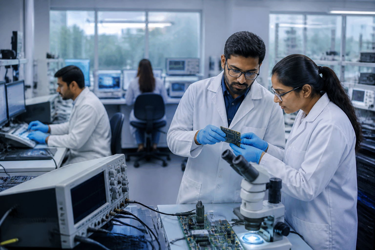
HCLTech has launched a semiconductor laboratory in Bengaluru with an investment of ₹185 crore, expanding its post-silicon engineering, testing and failure-analysis capabilities for domestic and international customers.
The 40,000-square-foot facility will support activities across research and development, pre-production and production qualification. HCLTech said the laboratory is designed to provide an integrated platform covering electrical validation, automated testing, qualification and failure analysis.
The facility is equipped with tools from Teradyne, Advantest, Keysight, Tektronix and Thermo Fisher Scientific. According to HCLTech, these capabilities are intended to support faster turnaround, improve quality and reduce complexity in the development and qualification of semiconductor parts.
The laboratory operates in line with HCLTech’s Spec2Parts business model, which brings together activities from design specifications through to finished semiconductor parts. The company said the unified setup will allow customers to access post-silicon engineering and advanced testing capabilities through a single platform.
“This facility reflects our deep commitment to investing in high-end engineering capabilities,” Hari Sadarahalli, corporate vice-president and global head of engineering and R&D services at HCLTech, said in a statement.
HCLTech said the Bengaluru laboratory will serve both domestic and international markets. The company described the facility as part of its global strategy to provide semiconductor solutions and strengthen India’s position in the sector. The announcement did not provide details on the number of employees, specific customer projects or an operational expansion timeline.
